Why It Matters
In context: As we approach the 2nm process node, some roadblocks are emerging that could further stagnate the already slow Moore’s Law progress. One challenge is how to efficiently distribute power to tens of billions of tiny transistors using copper wiring without eroding performance gains. Now, Applied Materials, a major supplier of semiconductor manufacturing equipment, believes it has the answer.
Last week, Applied Materials revealed its latest materials engineering solutions designed to enable copper wiring to scale down to 2nm dimensions and below while reducing electrical resistance and strengthening chips for 3D stacking.
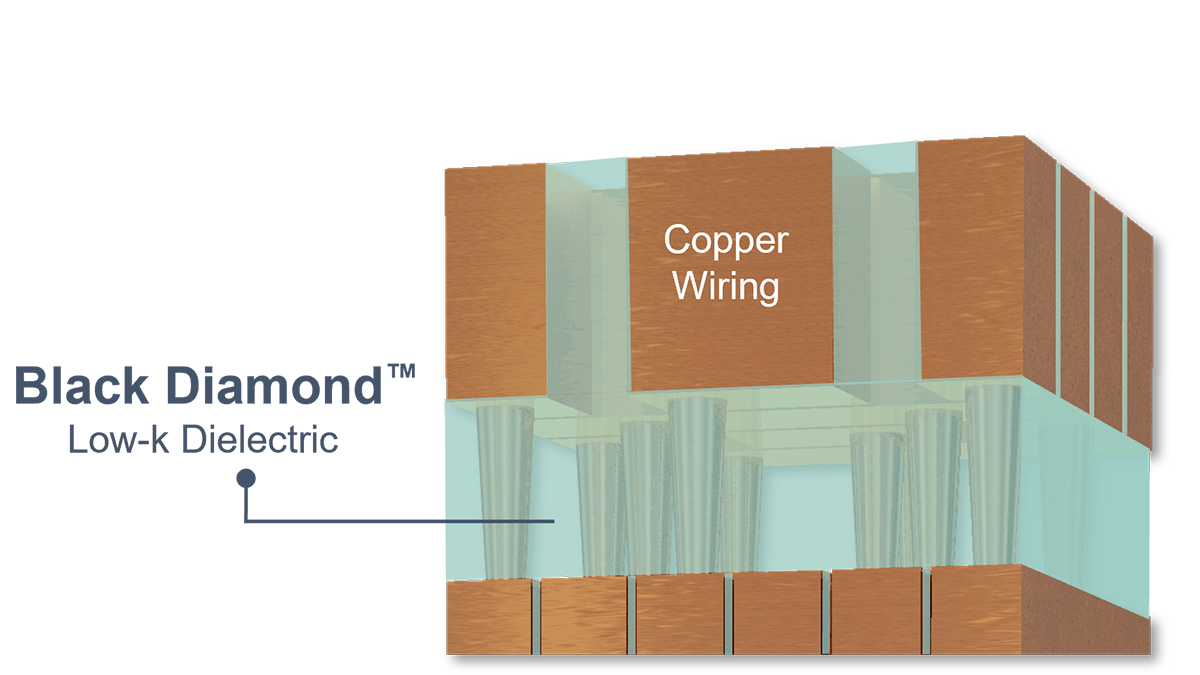
The company’s Black Diamond low-k dielectric material has been available since the early 2000s. It surrounds copper wires with a special film engineered to reduce the buildup of electrical charges that increase power consumption and cause interference between electrical signals.
Applied Materials has now introduced an enhanced version of Black Diamond, reducing the minimum k-value even further. This advancement enables copper wiring scaling to the 2nm node while increasing mechanical strength – a critical property for stacking multiple logic and memory dies vertically.
Scaling the copper wiring itself as dimensions shrink poses an enormous challenge. Today’s cutting-edge logic chips can pack over 60 miles of copper wires, crafted by etching trenches into the dielectric material and depositing an ultra-thin barrier layer to prevent copper migration. A liner layer aids copper adhesion before the final copper deposition fills the remaining space.
The barrier and liner layers consume an increasingly large percentage of the trench volume at 2nm dimensions and below, impacting copper fill and risking high resistance and reliability issues. Applied Materials has addressed this challenge with a new materials concoction.
Their latest Integrated Materials Solution (IMS) combines six core technologies into one high-vacuum system, featuring an industry-first pairing of ruthenium and cobalt to create an ultra-thin 2nm binary metal liner. This innovation allows a 33% reduction in liner thickness compared to previous generations, enhancing surface properties for seamless, void-free copper adhesion and reflow. The outcome is up to 25% lower electrical resistance in chip wiring to enhance performance and reduce power leakage.
Applied Materials states that leading logic chipmakers have already adopted its new copper barrier seed IMS with ruthenium CVD technology for 3nm chip production, with 2nm nodes anticipated to follow suit.
The company predicts that its total served available market for chip wiring solutions will increase from around $6 billion per 100,000 wafers today to over $7 billion with the introduction of backside power delivery schemes.